
RFID stands for Radio Frequency I identification technology, commonly known as electronic tags. RFID radio frequency identification is a non-contact automatic identification technology that automatically identifies target objects and obtains relevant data through radio frequency signals. The identification work does not require manual intervention and can work in various harsh environments. RFID technology can recognize high-speed moving objects and simultaneously recognize multiple tags, making operation fast and convenient.
The most basic RFID system consists of three parts: tags, readers, and antennas. A complete system also needs to have a data transmission and processing system. The basic working principle of RFID technology is not complicated: after the tag enters the magnetic field, it receives the RF signal emitted by the interpreter, and uses the energy obtained from the induced current to send product information stored in the chip, or actively sends a signal of a certain frequency; After the interpreter reads and decodes the information, it is sent to the central information system for relevant data processing.
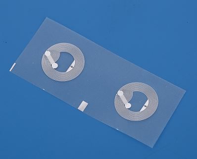
On the interconnection between printed antennas and chips, due to the high working frequency of RFID tags and the small and ultra-thin chips, the most suitable method is flip chip technology. It has the characteristics of high performance, low cost, miniaturization, and high reliability. To adapt to flexible substrate materials, the flip bonding material needs to use conductive adhesive to achieve the interconnection between chips and antenna pads. To achieve large-scale and low-cost production of flexible substrates, and to more effectively reduce production costs, adopting new methods for antenna chip interconnection is currently a hot research topic both internationally and domestically.
In order to adapt to smaller RFID chips and effectively reduce production costs, the current trend is to use bonding packaging between chips and antenna substrates, which is divided into two modules and completed separately. One specific approach is to manufacture large-sized antenna substrates and small substrates connecting chips separately. After chip mounting and interconnection are completed on the small substrates, the circuit is then connected to the large-sized antenna substrate through the adhesion of large solder pads. A similar method to dividing the packaging process into two modules as mentioned above is to first transfer the chip to a carrier that can evenly support the chip, and then flip the chip on the carrier onto the antenna substrate. In this method, the flip of the chip is achieved by flipping the carrier tape, simplifying the chip picking operation and thus achieving higher production efficiency.
RFID tags come in various packaging forms for different purposes, resulting in diverse packaging processes such as antenna manufacturing, bump formation, and chip bonding and interconnection.
(1) Antenna manufacturing
Winding antenna substrate (corresponding to lead bonding packaging)
Printed antenna substrate (corresponding to inverted chip conductive adhesive packaging)
Etched antenna substrate (corresponding to lead bonding packaging or module riveting packaging)
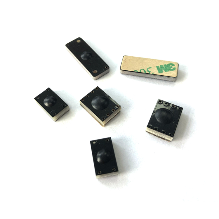
(2) Formation of convex points
The current characteristic of RFID tag products is a wide variety, but not every variety can form a scale. Therefore, adopting flexible manufacturing technology for convex points has the characteristics of low cost, high packaging efficiency, convenient and flexible use, simple process control, and high degree of automation. Not only can it solve the urgent problems of variable processing batch, high-density, and low-cost packaging in the microelectronics industry, but it also provides conditions for the flexible production of RFID tags that are currently booming.
(3) RFID chip interconnection methodOne of the main goals of RFID tag manufacturing is to reduce costs. Therefore, it is necessary to minimize the number of processes, choose low-cost materials, and reduce process time as much as possible.
There are three ways to interconnect the convex points of flip chip with flexible substrate pads: isotropic conductive adhesive (ICA) with bottom filling, anisotropic conductive adhesive (ACA, ACF), and non-conductive adhesive (NCA) directly pressing the protruding points of the nail head. In theory, priority should be given to NCA interconnection, which can be combined with adhesive protrusions to achieve low-cost manufacturing, but there are certain limitations and reliability.
The advantage of using ICA is low cost and no pressure is required for curing. The operation process steps are cumbersome and difficult to reduce costs. Usually, the curing time is long, making it difficult to improve production speed. In the form of first manufacturing a small substrate connecting the chip and then connecting it to a large-sized antenna substrate, the preferred method is to complete circuit conduction through ICA adhesion. Usually, low-cost and fast curing ACF and ACA are used. The specific method is to use ordinary stencil printing technology to apply a layer of ACA at the corresponding position of the antenna substrate solder pad, use an inverted chip mounting machine to place the chip in the corresponding position, and then heat press and cure it.
Another bonding method is to first manufacture the RFID module and then rivet it onto the antenna substrate for assembly.
From practical applications, electronic tags have various packaging forms that are not limited by standard shapes and sizes, and their composition varies greatly, even requiring special designs according to various requirements. At present, the sizes that have been applied range from ¥ 6mm to 76 × 45mm, and even smaller ones are made using micrometer scale chips, including antennas, which are only 0.4 × 0.4mm in size; The storage capacity ranges from small capacity models with read-only ID numbers ranging from 64-200 bits to large capacity models that can store tens of thousands of bits of data (such as EEPROM32Kbit); Packaging materials range from self-adhesive to plastic for injection molding. For various packaging forms of electronic tags, their materials, composition, etc. are different.
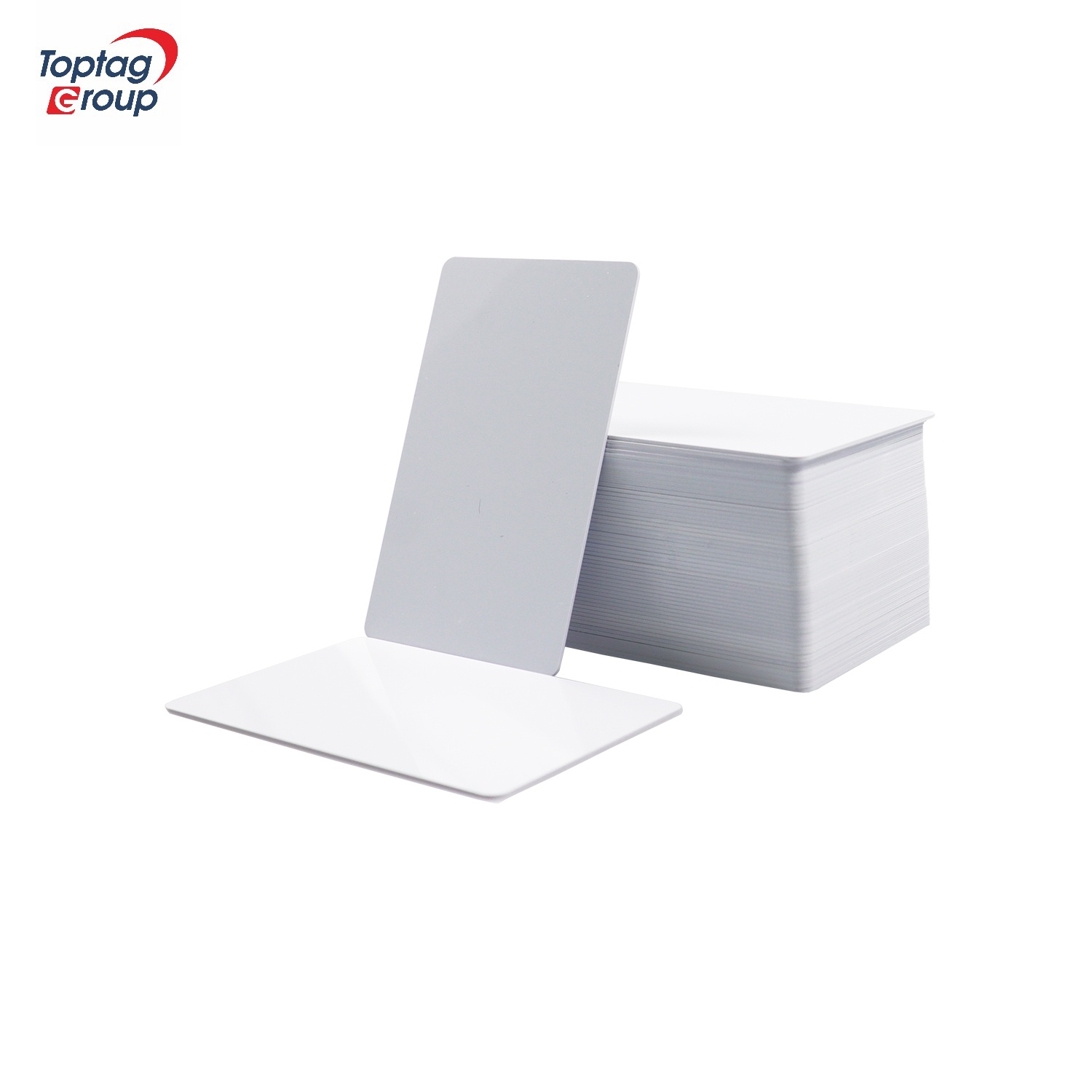
(1) Card type (PVC, paper, others)
Laminated, there are two types: melt pressing and seal pressing. Melt pressing is made by heating and pressing the INLAY sheet in the center layer and the upper and lower PVC sheets. PVC material is fused with INLAY and then punched to the size specified in ISO7816. When the chip adopts a transponder, the chip protrudes above the antenna plane (with an antenna thickness of 0.01-0.03mm), and another lamination method, namely sealing, can be used. At this time, the substrate is usually PET or paper, and the chip thickness is usually 0.20-0.38mm. When making cards and packaging, only PVC is sealed around the antenna, not fused, and the chip part is not compressed, which can avoid the chip being crushed. Gluing type, using paper or other materials to bond the upper and lower materials of the transponder together through cold glue, and then mold and cut them into various sizes of cards.
(2) Label class
Adhesive type, the finished product can be made into a manual or label removal form by a labeling machine, and is the most commonly used mainstream product. That is, an electronic label is attached to the back of the trademark and directly affixed to the marked object. Such as luggage tags for aviation, tags for pallets, etc. Hang tag style, corresponding to clothing and items using hang tag products, characterized by compact size and recyclability.
(3) Alien class
Metal surface setting type, most electronic tags are affected to varying degrees by the metal and cannot function properly. These types of labels have been specially processed and can be placed on metal for reading and writing. Used for the surface of various metal components such as pressure vessels, boilers, fire equipment, etc.
Wrist strap type, can be disposable (such as for medical purposes) or reused (such as in amusement parks).
Animal and plant use type, packaging form can be injection type glass tube, hanging ear tag, buckle type foot ring, etc. Electronic tag technology has gained increasing market recognition due to its breakthrough technological characteristics and wide applicability.
With the further improvement of chip manufacturing and packaging processes, as well as the increasing maturity of packaging equipment and materials, electronic tags will undoubtedly be more suitable for our needs.
Related Products