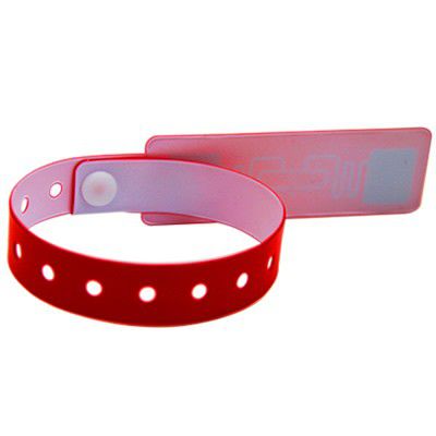

RFID Inlay Tag — The Smart Layer Before the Smart Card
For card manufacturers, security printers, and access control OEMs who laminate finished cards in-house but need a reliable, customisable source for the embedded electronics — the layer that actually carries the chip, the antenna, and the data.
An RFID Inlay Tag is not a finished card. It is a semi-finished PVC sheet — typically 0.4 mm to 0.5 mm thick — with RFID chips and wire-embedded or etched-aluminium antenna coils precisely positioned inside a cavity grid. When a card manufacturer takes this sheet and sandwiches it between two printed PVC overlay sheets under heat and pressure, the result is a finished ISO 7810 CR80 card. The inlay is the invisible infrastructure. Every tap-to-pay bank card, every hotel key, every transit pass, every access control badge — they all start as an inlay sheet sourced from a specialist manufacturer, not from the printer that personalises the surface.
Our Shenzhen facility produces these sheets across LF (125 kHz), HF (13.56 MHz), and UHF (860–960 MHz) bands, with any chip protocol the end application demands. Sheet dimensions, cavity counts per sheet, antenna geometry, and chip placement are all configurable to match your lamination tooling. No forced standard. No “this is our only layout.” The inlay is built around your production line — not the other way around.

Why Card Manufacturers Buy Inlays Instead of Making Them
The economics of in-house RFID antenna production are punishing. A copper-wire embedding machine — the type that ultrasonically lays 112-micron copper wire into a PVC substrate following a CNC-generated antenna pattern — costs north of USD 180,000 before installation. Add a chip-bonding station (USD 45,000–80,000), a laminator stack (USD 120,000), and the cleanroom environment both require, and the upfront capex crosses USD 400,000 — before a single sheet ships. Then there is the engineering overhead: antenna impedance must be tuned to ±2 Ω of the chip’s specified load for optimal read range, and every chip protocol (MIFARE Classic vs. MIFARE Ultralight vs. ICODE SLIX vs. Alien Higgs-3) requires a different antenna geometry because each chip presents a different input capacitance at 13.56 MHz.
Buying finished inlay sheets from a dedicated manufacturer collapses that capex into a per-unit variable cost. A card manufacturer that purchases 100,000 inlay sheets per year at $1.20 each spends $120,000 — less than the cost of the wire-embedding machine alone — and receives QC-certified, impedance-matched, chip-bonded sheets ready for lamination. The manufacturer’s capital stays in printing presses, laminators, and personalisation equipment — the things that actually differentiate a finished card. The inlay is a commodity component, and commodities are almost always cheaper to buy than to make.
This is the same logic that made PCB fabrication a specialised industry forty years ago. No consumer electronics company etches its own boards. No card manufacturer should embed its own antennas — unless it ships over five million cards a year. Below that threshold, buying inlays is not a cost; failing to buy them is an unforced error on the balance sheet.
Chip Flexibility — One Supplier, Any Frequency, Any Protocol
Because the inlay is purely the electronic layer — no printing, no personalisation, no cosmetic overlay — the only variable that matters is the silicon inside. Our inlay sheets accept any RFID chip, on any frequency, without changing the sheet tooling. The cavity geometry is chip-agnostic; the antenna layout is configured per chip specification.
LF 125 kHz — EM4200, ATA5577, T5577
For access control systems that still run on legacy 125 kHz readers — a large installed base across Eastern Europe, Southeast Asia, and South America. Copper coil antenna wound to match the chip’s resonant frequency. Typical read range: 2–5 cm on a standard desktop reader. Used in proximity door cards, employee ID badges, and parking access tokens.
HF 13.56 MHz — MIFARE, ICODE, NTAG-compatible, Fudan FM11
The largest category by volume. MIFARE Classic 1K and 4K for transit and access control. MIFARE Ultralight and NTAG-compatible for single-trip tickets and event passes. ICODE SLIX for library and supply chain asset tracking (ISO 15693). Fudan FM11RF08 for cost-sensitive mass-transit deployments. Antenna can be copper-wire-embedded or etched aluminium on PET, depending on read-range requirements and unit-cost targets. The choice of substrate — PVC or PET — also affects lamination temperature compatibility: PET withstands higher lamination temperatures, making it suitable for polycarbonate composite cards.
UHF 860–960 MHz — Alien Higgs-3/4, Impinj Monza R6/M730
For logistics, warehouse inventory, and vehicle identification where read ranges of 3–10 metres are required. UHF inlays use a dipole antenna geometry — typically an aluminium-etched pattern on a PET substrate — rather than a copper coil. The sheet layout for UHF differs from HF because the antenna footprint is larger, reducing the number of cavities per sheet. Standard UHF inlay sheets yield 18–24 cavities per A4-sized sheet, compared to 48–64 for HF.

Customisation That Card Manufacturers Actually Need
Standardisation is for retail. In industrial B2B, every customer’s lamination tooling is slightly different, and an inlay sheet that does not fit the tooling is waste. Our customisation scope covers five variables, none of which increase MOQ beyond 500 sheets:
Sheet dimensions
Standard offering is A4 (210 × 297 mm) and 3-up (3 × 8 cavity grid, 24 cavities per sheet). Custom sheet sizes — including half-A4 for smaller laminators and A3 for high-throughput roll-to-roll systems — are produced on the same tooling with insert swaps that take under 90 minutes. No new mould charge, no engineering fee.
Cavity grid layout
The number of chips per sheet is determined by cavity spacing, which is determined by the customer’s lamination platen geometry. A 3 × 8 grid (24-up) is the most common for CR80 cards. 4 × 8 (32-up) for thin cards. 5 × 10 (50-up) for high-density production lines. Cavity pitch tolerance is ±0.15 mm across the full sheet — verified on a coordinate measuring machine before every batch ships.
Antenna design
Copper-wire-embedded antennas are the default for HF and LF. Wire diameter: 112 microns standard, 80 microns for thin-card applications. Turns: 4–7 depending on chip inductance requirements. Etched-aluminium antennas on PET substrate are available for UHF and for HF applications requiring thinner total card thickness. For customers with an existing antenna design file, we accept Gerber RS-274X format and produce a first-article sheet within five working days.
Chip placement and bonding
Chip-to-antenna bonding is performed on an automated flip-chip bonder using anisotropic conductive paste (ACP) cured under precisely controlled temperature and pressure. Bond strength is verified on a pull tester sampling 5% of every batch — minimum 3.5 N before the chip separates from the antenna pad. For dual-interface chips (contact + contactless, e.g. Infineon SLC37), the bonding station also connects the contact pads to the ISO 7816 contact plate position.
Material composition
Standard substrate is virgin PVC with a Vicat softening point of 75°C — compatible with most hot-lamination presses. PET substrate available for polycarbonate composite cards requiring lamination temperatures above 130°C. All materials are RoHS-compliant and traceable to the resin supplier’s certificate of analysis. REACH compliance documentation available on request for EU importers.
Manufacturing — What Happens on the Production Floor
The inlay production line runs on a campus that also houses our finished-card lamination and personalisation lines — but the inlay line is physically separated, with its own climate control (22°C ± 1°C, 45% ± 5% RH) because PVC substrate expansion and copper wire impedance both drift with ambient temperature.
The process starts with a PVC core sheet fed into a TAL 2000 wire-embedding machine — a German-made ultrasonic wire-laying system that embeds 112-micron enamel-coated copper wire into the PVC surface following a CNC-generated antenna pattern. The wire is laid at 300 mm/s, ultrasonically bonded to the substrate so it sits flush with the surface rather than protruding — critical because any raised wire creates an air pocket during lamination, and air pockets are the primary cause of card delamination in the field.
The embedded sheet then moves to a Datacon 8800 flip-chip bonder. Each RFID chip is picked from a waffle tray, aligned to the antenna pads with a vision system accuracy of ±10 microns, and bonded using ACP cured at 180°C for 12 seconds. The bonder processes 4,500 chips per hour — a single machine handles the output of four wire embedders.
After bonding, every cavity on every sheet is tested in a tunnel reader that excites the antenna at the chip’s resonant frequency and verifies both the UID readback and the signal amplitude. A cavity that reads back a UID but at 60% of the expected amplitude passes functional QC but is flagged for root-cause analysis — the most common cause is a partially delaminated antenna bond that weakens the magnetic coupling. Flagged sheets are quarantined and released only after a batch-level investigation confirms the root cause is not systematic.
 Dedicated inlay production line. Climate-controlled at 22°C ± 1°C. TAL 2000 wire embedding → Datacon 8800 chip bonding → cavity-level electrical test → sheet-level visual inspection.
RFID Inlay Tag Technical Specifications
| Parameter | Value |
|---|---|
| Product type | Semi-finished PVC inlay sheet with embedded RFID chip and antenna |
| Frequency bands | LF 125 kHz / HF 13.56 MHz / UHF 860–960 MHz |
| Supported chips | EM4200, ATA5577, T5577, MIFARE Classic 1K/4K, MIFARE Ultralight, NTAG-compatible (NXP NTAG213/215/216), ICODE SLIX, Fudan FM11RF08, Alien Higgs-3/4, Impinj Monza R6/M730 — custom chips on request |
| Antenna type | Copper wire embedded (112-micron enamel-coated Cu) or aluminium etched on PET |
| Sheet dimensions | Standard: A4 (210 × 297 mm), 3-up (3×8 grid). Custom: half-A4, A3, or customer-specified |
| Sheet thickness | 0.40 mm ± 0.03 mm (standard); 0.50 mm ± 0.03 mm (thick); 0.35 mm ± 0.03 mm (thin-card) |
| Cavity configurations | 3×8 (24-up), 4×8 (32-up), 5×10 (50-up), or custom grid |
| Cavity pitch tolerance | ±0.15 mm across full sheet |
| Chip bonding | Flip-chip ACP (anisotropic conductive paste), cured at 180°C / 12 sec |
| Bond strength | ≥ 3.5 N (pull test, 5% batch sampling) |
| Substrate material | Virgin PVC (Vicat 75°C) or PET (for polycarbonate composite cards, Vicat >130°C) |
| Operating temperature | −25°C to +70°C (PVC); −40°C to +85°C (PET) |
| QC sampling rate | 100% cavity-level electrical test + 5% pull-test + visual inspection under D65 light booth |
| Certifications | ISO 9001 (factory), RoHS (materials), REACH documentation on request |
| MOQ | 500 sheets (standard configuration); 1,000 sheets (custom antenna design) |
| Lead time | 7–12 working days (standard); 15–20 working days (custom antenna or chip) |
| Packing | 100 sheets / vacuum-sealed anti-static bag; 5 bags / carton |
Quality Assurance — Why Every Cavity Gets Tested
In finished-card production, a defective inlay is discovered only after lamination, printing, and personalisation — when the card has already accumulated the full manufacturing cost. At that point, the loss is not the $1.20 inlay cost; it is the $3.50 fully produced card, plus the labour to identify and re-run the defective unit, plus the shipping delay if the order was against a tight deadline.
This is why we test 100% of cavities on 100% of sheets before the inlay leaves the factory. The tunnel reader excites each antenna at the chip’s resonant frequency and logs three data points per cavity: UID readback (pass/fail), signal amplitude (in mV, benchmarked against the batch mean), and resonance frequency shift (in kHz, indicating potential antenna geometry drift). A sheet that fails any cavity is quarantined; a batch where more than 0.5% of cavities fail triggers a full production-line stop and root-cause investigation.
For customers who require traceability, every sheet ships with a QR-coded lot label that links to a digital QC dossier containing: batch production date, wire-embedding machine operator ID, chip-bonding station ID, ACP lot number, tunnel reader calibration date, and the cavity-level test log in CSV format. This is the same level of traceability that payment-card manufacturers require under EMVCo security audit guidelines — available to any customer, on any order size, at no additional charge.

Supply Chain Logic — When Low MOQ Matters More Than Low Unit Price
Most inlay manufacturers set MOQs at 5,000 to 10,000 sheets. This is not because the production process requires it — a wire-embedding machine can switch antenna patterns in under two hours — but because high-MOQ factories are optimised for the payment-card industry, where a single order from a bank typically runs 500,000 to two million cards. A 500-sheet order disrupts that optimisation.
Our production line is architected differently. The TAL 2000 wire embedder stores 200 antenna patterns in onboard memory and switches between them with a software command rather than a mechanical tooling change. The Datacon bonder’s waffle-tray feeder accepts mixed chip types in the same run. This means a 500-sheet order for MIFARE Classic 1K inlays can run immediately after a 2,000-sheet order for ICODE SLIX inlays with a changeover time under 90 minutes. There is no minimum economic batch size — only a minimum practical one, and 500 sheets is that floor.
For a card manufacturer testing a new end-customer deployment — say, a university piloting MIFARE-based student ID cards across 5,000 students — 500 inlay sheets producing 12,000 cavities is exactly the right quantity. It is enough for the pilot, enough for spares, and small enough that if the deployment requirements change (different chip, different frequency), the manufacturer is not sitting on 8,000 sheets of unusable inventory. Low MOQ is not a discount strategy. It is a risk-management strategy, and for industrial buyers, managing supply-chain risk is the job.
Global Deployments — Where Our Inlays End Up
RFID Inlay Tag sheets from this line are embedded in finished cards deployed across more than forty countries. A national transit authority in Central Asia issues 4.2 million MIFARE Classic-based fare cards annually — the inlays for those cards ship from this factory in 210,000-sheet lots, four times a year. A European security printer producing access control badges for data centres uses EM4200 LF inlays configured in a 4 × 8 grid to match their Heidelberg laminator platen dimensions. A Southeast Asian loyalty-card programme for a fuel-station chain runs on NTAG-compatible HF inlays in a custom half-A4 sheet size — because their laminator is a legacy machine originally designed for magnetic-stripe cards, retrofitted with a smaller platen.
In every case, the inlay sheet was configured to the customer’s existing tooling, not the other way around. This is the difference between a component supplier and a commodity supplier. A commodity supplier sells what it makes. A component supplier makes what the customer needs to build.
Frequently Asked Questions
What is the difference between an RFID Inlay Tag and a finished RFID card?
An RFID Inlay Tag is the middle layer — the PVC sheet carrying the chip and antenna — without printed overlay sheets, without personalisation (no printed cardholder name, no photo, no serial number), and without lamination. It is a component, not a finished product. Card manufacturers buy inlay sheets, sandwich them between printed PVC overlays, laminate under heat and pressure, then die-cut to CR80 dimensions and personalise. The inlay provides the electronics; the overlay provides the graphics; the lamination fuses them into a single card body.
Can you embed a chip that is not on your standard list?
Yes. If the chip is available on the open market and its datasheet specifies the bonding pad layout and antenna impedance requirements, we can design an antenna for it and bond it into an inlay sheet. First-article turnaround for a new chip: five to eight working days from receipt of the chip samples or the full datasheet. There is no engineering fee for this service — it is absorbed into the per-sheet pricing because custom chip support is the standard operating model, not an exception.
What if I need only 200 sheets for a small pilot?
The line minimum is 500 sheets, but we can split a single 500-sheet order across two chip types (e.g. 250 sheets MIFARE Classic + 250 sheets NTAG-compatible) if both use the same frequency band and cavity layout. This effectively gives you a 250-sheet effective MOQ per chip variant. For evaluation before committing to a production order, we ship five free sample sheets in any configuration within five business days to any verified company address.
Do you provide the lamination overlay sheets as well?
We produce finished cards on a separate production line, so yes — if you prefer to receive fully laminated, die-cut, and personalised cards rather than inlay sheets, that is available. But most card manufacturers prefer to laminate and personalise in-house because it gives them control over the printing quality, the overlay material (matte vs. gloss vs. signature panel), and the personalisation method (thermal transfer vs. retransfer vs. laser engraving). We ship inlays to customers who want to control those variables themselves.
How are the sheets packed for international shipping?
Vacuum-sealed anti-static bags, 100 sheets per bag, with a silica-gel desiccant pack inside. Five bags per export-grade double-wall corrugated carton. The vacuum seal prevents PVC sheet warping from humidity exposure during ocean freight; the anti-static bag prevents ESD damage to exposed antenna pads. Every carton carries a ShockWatch indicator and a tilt indicator — if either is triggered during transit, the receiving party can refuse the shipment before opening, and we file the claim with the carrier directly.
Request Free Engineering Samples
Tell us your chip protocol, frequency band, sheet dimensions, and cavity grid layout — or send us your lamination tooling specifications and we will propose the optimal inlay configuration. Five sample sheets ship within five business days to any verified company address worldwide. No commitment, no engineering fee, no minimum beyond the sample request itself.
Email: [email protected] | WhatsApp: +852 5989 6589 | WeChat: 147891664
Also see our RFID card manufacturing capabilities for finished-card production options, including lamination, die-cutting, and personalisation services.